Recent News
May 8 seminar: Gangadharan Esakk
May 5, 2026
May 1 seminar: Alexander Scheinker
April 29, 2026
April 24 seminar: Jon Loftin
April 22, 2026
April 17 seminar: Abee Alazzwi
April 15, 2026
News Archives
Seminar: Shashank Sharma
March 21, 2024

March 22, 2024
Novel Processes for Advanced Nanoelectronic Devices
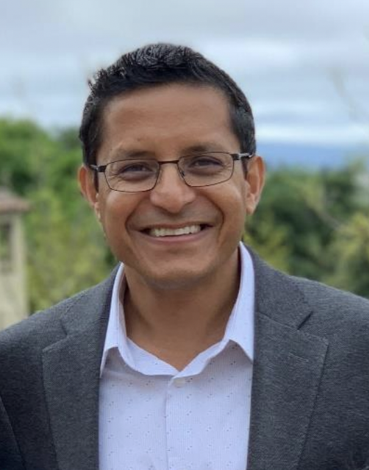
Shashank Sharma, Applied Materials, Santa Clara, CA
3:00 pm, ECE Building, Room 118
Online Guests: Contact Prof. Osiński <osinski@chtm.unm.edu> for a Zoom link
Abstract: Relentless scaling over the past several decades of semiconductor devices has been driven by performance, power, density, and cost requirements. Semiconductor industry has been successfully meeting these requirements with continued innovations in design, integration, and materials engineering. Logic transistor technology transitioned from planar geometry to 3D geometries such as FinFETs and horizontal gate all around, while introducing numerous new materials and processes across front end of the line all the way into back end of the line. Memory devices on the other hand have also seen integration in third dimension both in NAND and DRAM. This talk reviews some of the key challenges introduced by the new device architectures and various materials processing innovations that enable continued scaling.
Bio: Dr. Shashank Sharma holds the CTO position in Front End Products business unit in Semiconductor Products Group at Applied Materials. He has more than 20 years experience in the semiconductor industry, with the past >12 years at Applied Materials, developing advanced semiconductor process technologies in the areas of thermal and activated species treatment. He has authored/co-authored more than 60 publications and is credited with more than 24 granted patents. Dr. Sharma received his M.S. and Ph.D. degrees in Chemical Engineering from the University of Louisville, Kentucky in 2000 and 2003, respectively.
